février 26, 2024
4722
Integrated circuits (ICs), also known as microchips or chips, have revolutionized the field of electronics since their invention in 1958. These miniature electronic circuits, composed of semiconductor materials like silicon, contain various electronic components such as transistors, resistors, capacitors, and diodes, all etched onto a single chip. This integration allows for compact, reliable, and high-performance electronic devices across a wide range of applications. In this article, we explore the definition, function, types, and fabrication of integrated circuits, shedding light on their significance in modern technology.
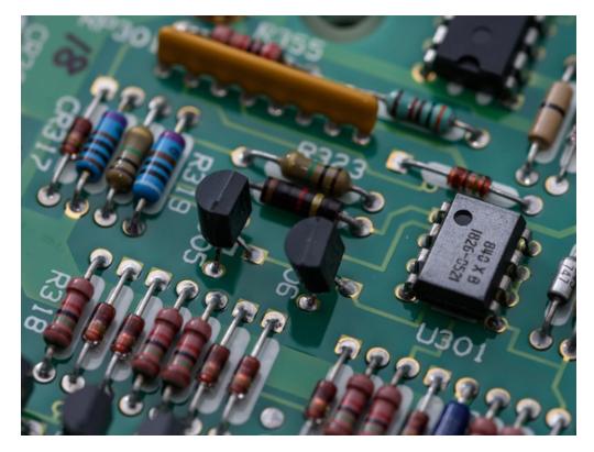
Integrated circuits (ICs), also known as microchips or simply chips, are miniature electronic circuits that are composed of semiconductor materials, such as silicon. These circuits are etched or imprinted onto a tiny chip of semiconductor material, typically silicon. Integrated circuits contain electronic components such as transistors, resistors, capacitors, and diodes, as well as interconnections that allow them to perform various functions, including amplification, switching, and digital computation.
The integration of multiple electronic components onto a single chip greatly reduces the size and cost of electronic devices while increasing their reliability and performance. Integrated circuits are used in a wide range of applications, including computers, smartphones, medical devices, automotive systems, and many other electronic devices. They are essential building blocks of modern electronics and have revolutionized the way electronic systems are designed and manufactured.
Integrated circuit packaging refers to the process of enclosing a semiconductor die (the silicon wafer containing the integrated circuit) within a protective housing or package. The packaging serves several important functions, including providing mechanical support, protecting the die from environmental factors such as moisture and temperature fluctuations, and facilitating electrical connections between the integrated circuit and external components or circuitry.
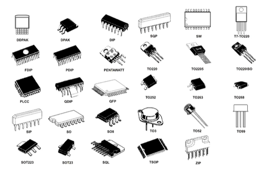
Dual in-line package (DIP): This is one of the earliest forms of IC packaging, featuring two parallel rows of pins along the sides of the package.
Quad flat package (QFP): This package has gull-wing shaped leads extending from all four sides of the package, allowing for higher pin counts and improved thermal performance compared to DIP.
Ball grid array (BGA): In BGA packages, solder balls are arranged in a grid pattern on the underside of the package, providing a high-density interconnection solution suitable for modern integrated circuits with large numbers of I/Os.
Chip scale package (CSP): CSPs are designed to be nearly the same size as the semiconductor die itself, minimizing the footprint of the package and enabling highly compact electronic devices.
System-in-package (SiP): SiP technology involves integrating multiple ICs or other components within a single package, allowing for increased functionality and reduced system size.
IC packages are typically made from materials such as plastic, ceramic, or metal, depending on factors such as cost, performance requirements, and application-specific considerations.
Advanced packaging technologies may also incorporate materials with special properties, such as those designed to enhance thermal conductivity or provide improved electrical performance.
The packaging process involves several steps, including die attach, wire bonding or flip-chip bonding, encapsulation, and final testing.
During die attach, the semiconductor die is bonded to the package substrate using conductive adhesive or solder.
Wire bonding involves connecting the bond pads on the die to the package leads using thin wires made of gold, aluminum, or copper.
In flip-chip bonding, the die is flipped upside down and its bond pads are directly connected to the package substrate using solder bumps.
Encapsulation involves covering the die and wire bonds with a protective material, such as epoxy resin, to provide mechanical protection and environmental sealing.
Advanced packaging technologies, such as wafer-level packaging (WLP), 3D packaging, and fan-out wafer-level packaging (FOWLP), enable further miniaturization, increased performance, and enhanced functionality.
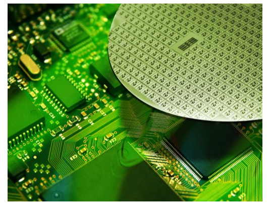
An integrated circuit wafer, often simply referred to as a silicon wafer, is a thin, circular substrate made of semiconductor material, typically silicon, on which multiple integrated circuit chips are fabricated simultaneously. These wafers serve as the foundation for the manufacturing process of integrated circuits (ICs).
Silicon is the most commonly used material for integrated circuit wafers due to its abundance, high purity, and favorable semiconductor properties. Other materials, such as gallium arsenide (GaAs) and silicon carbide (SiC), are also used for specialized applications.
Integrated circuit wafers come in various sizes, with diameters ranging from a few inches to over a foot. The most common sizes used in semiconductor manufacturing facilities are 150mm (6 inches), 200mm (8 inches), and 300mm (12 inches). Larger wafer sizes enable higher throughput and increased efficiency in the fabrication process.
Integrated circuit codes, also known as IC part numbers, are alphanumeric designations assigned to individual integrated circuit chips. These codes are crucial for identification, classification, and specification purposes, helping users discern the type, functionality, and manufacturer of the IC. Typically, IC codes consist of several components.
Firstly, they often incorporate a manufacturer code, indicating the company that produced the IC. Secondly, they specify the device type, such as microcontroller, memory chip, or analog/digital IC, providing insights into the IC's primary function.
Additionally, IC codes may include information about the series or family of the IC, aiding in differentiation between variations of the same type. Furthermore, they may indicate the package type or form factor of the IC, facilitating appropriate selection for specific applications.
Moreover, IC codes might contain details regarding functionality, specifications, or performance characteristics, such as memory capacity, operating voltage, or speed grade. In some cases, they may also incorporate a revision or date code, providing insights into the manufacturing date or revision level.
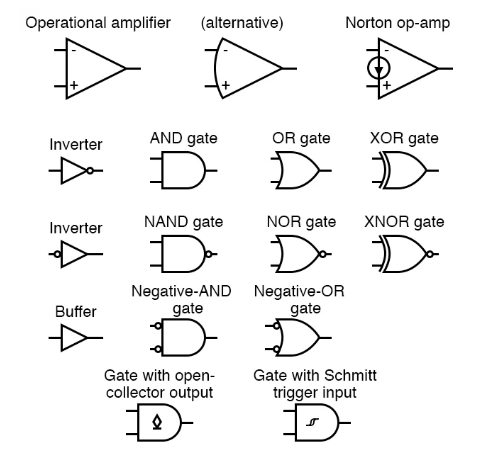
Analog ICs are designed to process continuous signals and perform functions such as amplification, filtering, and signal conditioning. They are used in applications like audio amplifiers, radio frequency (RF) circuits, sensors, and power management.
Digital ICs operate on discrete binary values and are used in digital electronics to perform logic operations, data processing, and control functions. Examples include microprocessors, memory chips, digital signal processors (DSPs), and field-programmable gate arrays (FPGAs).
Mixed-signal ICs integrate both analog and digital functions on the same chip, enabling the processing of both analog and digital signals within a single device. They are used in applications such as data conversion (ADCs and DACs), communications, and sensor interfaces.
Microcontrollers are specialized digital ICs that integrate a central processing unit (CPU), memory, input/output ports, and other peripherals on a single chip. They are commonly used in embedded systems to control and manage functions in devices such as microcontrollers, automotive systems, and home appliances.
Memory ICs store and retrieve data in digital devices and are available in various types, including random-access memory (RAM), read-only memory (ROM), electrically erasable programmable read-only memory (EEPROM), and flash memory. They are used in computers, smartphones, digital cameras, and other electronic devices.
RF ICs are optimized for radio frequency (RF) applications and are used in wireless communication systems, including cellular networks, Wi-Fi, Bluetooth, and RFID devices. They include RF transceivers, power amplifiers, frequency synthesizers, and RF front-end modules.
Power management ICs regulate and control the supply and distribution of power within electronic systems. They include voltage regulators, DC-DC converters, battery management ICs, and power switches, and are used in devices ranging from smartphones and laptops to industrial machinery and renewable energy systems.
Sensor ICs interface with various types of sensors to measure physical parameters such as temperature, pressure, motion, and light. They include sensor signal conditioning circuits, amplifiers, and analog-to-digital converters (ADCs) and are used in applications such as environmental monitoring, healthcare, automotive systems, and industrial automation.
Integrated circuit (IC) fabrication, also known as semiconductor manufacturing or semiconductor fabrication, is the process of creating integrated circuits on silicon wafers using various semiconductor manufacturing techniques.
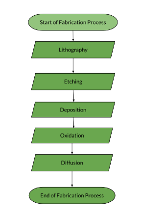
The fabrication process begins with the preparation of silicon wafers. These wafers are typically made from high-purity silicon crystals and undergo several cleaning and polishing steps to achieve a smooth and uniform surface.
The silicon wafers are thoroughly cleaned to remove any contaminants or particles that could affect the fabrication process. This step is crucial for ensuring the quality and reliability of the fabricated ICs.
Photolithography is a key step in IC fabrication, where a pattern of circuit features is transferred onto the surface of the silicon wafer. This process involves coating the wafer with a photosensitive material (photoresist), exposing it to ultraviolet (UV) light through a photomask containing the desired circuit pattern, and then developing the photoresist to reveal the pattern on the wafer.
Etching is used to remove material from the silicon wafer based on the pattern defined by photolithography. Wet etching involves using chemical solutions to selectively dissolve the exposed areas of the wafer, while dry etching uses plasma or reactive gases to remove material through physical or chemical processes.
Doping is the process of introducing impurities into the silicon wafer to modify its electrical properties. This is achieved by selectively diffusing dopant atoms (such as boron or phosphorus) into the wafer or by ion implantation, where dopant ions are accelerated and implanted into the wafer's surface.
Deposition involves depositing thin films of materials onto the surface of the silicon wafer to create various layers of the integrated circuit. This can be done using techniques such as chemical vapor deposition (CVD), physical vapor deposition (PVD), or atomic layer deposition (ALD).
Additional lithography steps may be performed to define the features of different layers in the IC, such as metal interconnects, contacts, and vias. This involves repeating the photolithography process with new photomasks to create the desired patterns on each layer.
After doping and deposition steps, the wafer may undergo annealing processes to activate dopants, repair crystal defects, and improve the electrical properties of the fabricated devices.
Metal layers are deposited and patterned to create interconnects between different components and layers of the IC, allowing electrical signals to flow between them.
After fabrication, the individual ICs on the wafer are tested for functionality and quality. The wafer is then diced into individual chips, which are packaged into protective housings or packages. Final testing is performed on the packaged ICs before they are shipped for use in electronic devices.
While all microprocessors are integrated circuits, not all integrated circuits are microprocessors. Integrated circuits encompass a broader category of miniaturized electronic circuits, whereas microprocessors specifically refer to ICs designed to function as the CPU in computing and electronic systems.
In summary, integrated circuits are electronic circuits fabricated using semiconductor materials, with multiple components and interconnections integrated onto a single chip. Semiconductors, on the other hand, are the materials used as the foundation for fabricating integrated circuits and other electronic devices, exhibiting unique electrical properties that enable their functionality.
Computers and Mobile Devices
Communication Systems
Consumer Electronics
Automotive Electronics
Industrial Automation
Medical Devices
Aerospace and Defense
Energy and Power Systems
IoT (Internet of Things)
While integrated circuits are the functional core of electronic devices, providing specific electronic functions, printed circuit boards serve as the physical platform for mounting and interconnecting electronic components, including integrated circuits, to form complete electronic systems. Together, ICs and PCBs work in tandem to enable the functionality, connectivity, and operation of electronic devices across a wide range of applications.
While transistors are individual semiconductor devices used to control or amplify electronic signals within electronic circuits, integrated circuits are complete electronic circuits fabricated onto a single semiconductor substrate, containing multiple transistors and other components interconnected to perform specific functions. Integrated circuits often incorporate transistors along with other components to achieve complex electronic functions within a compact package.
Integrated circuits have transformed the landscape of electronics, enabling the development of increasingly powerful, compact, and versatile electronic devices. From computers and smartphones to automotive systems and medical devices, ICs play a crucial role in virtually every aspect of modern life. As semiconductor technology continues to advance, integrated circuits will likely become even smaller, more efficient, and more specialized, further pushing the boundaries of what is possible in the realm of electronics.
What is application specific Integrated Circuit
An Application-Specific Integrated Circuit (ASIC) is a type of integrated circuit (IC) that is designed and fabricated for a specific application or purpose. Unlike general-purpose ICs, which are versatile and can be used in a wide range of applications, ASICs are customized to meet the exact requirements of a particular application, providing optimized performance, power efficiency, and cost-effectiveness.
ASICs are commonly used in scenarios where off-the-shelf solutions are either unavailable or unsuitable due to specific performance, power, or size constraints. These circuits are tailored to perform specific functions or tasks within a system, offering advantages such as higher performance, lower power consumption, and smaller form factors compared to general-purpose alternatives.
How do Integrated Circuits work
Integrated circuits (ICs) work by integrating multiple electronic components onto a single semiconductor substrate or chip, enabling the execution of various electronic functions within a compact and interconnected package.
What is Integrated Circuit design
Integrated circuit (IC) design is the process of creating the layout and functionality of an integrated circuit, which involves designing the electronic components and interconnections that make up the circuit. IC design encompasses several stages, including conceptualization, specification, logic design, physical design, verification, and testing.
Where was the Integrated Circuit invented
The integrated circuit (IC) was invented in the United States. The development of the integrated circuit is credited to Jack Kilby, who was working at Texas Instruments (TI) at the time. Kilby's breakthrough occurred in 1958 when he successfully demonstrated the first working integrated circuit. He developed the concept of integrating multiple electronic components onto a single semiconductor substrate to create a complete electronic circuit.
When was the Integrated Circuit invented
The integrated circuit (IC) was invented in 1958.
Where were the first Integrated Circuits used
The first integrated circuits (ICs) were primarily used in military and aerospace applications.
Who developed Integrated Circuit
Jack Kilby: Jack Kilby, an engineer at Texas Instruments (TI), is credited with inventing the integrated circuit in 1958. He developed the concept of integrating multiple electronic components onto a single semiconductor substrate to create a complete electronic circuit. Kilby's breakthrough occurred when he successfully demonstrated the first working integrated circuit on September 12, 1958.
Robert Noyce: Robert Noyce, a physicist and co-founder of Fairchild Semiconductor, also independently developed the integrated circuit in 1958. Noyce's approach involved using silicon as the semiconductor material and creating a planar integrated circuit. His design, which used a thin layer of oxide to electrically isolate components, became known as the planar process. Noyce's work laid the foundation for the mass production of integrated circuits.