janvier 31, 2024
5566

NMOS (N-Metal-Oxide-Semiconductor) transistors are key components in semiconductor devices and integrated circuits. In order to understand how it works, it is necessary to understand the basic concepts of semiconductor physics.
MOS transistor is a general term that includes P-type (PMOS) and N-type (NMOS) transistors. These transistors are the basic building blocks of integrated circuits.
In the manufacturing of P-type semiconductors, P-type semiconductors are formed by adding trace amounts of trivalent elements (such as boron, indium, gallium, aluminum, etc.) to single crystal silicon. In the manufacturing of N-type semiconductors, N-type semiconductors are formed by adding trace amounts of pentavalent elements (such as phosphorus and antimony). These added elements change the conductive properties of silicon.
NMOS transistors are manufactured using N-type semiconductor materials. The structure of a transistor consists of a metal gate separated from the semiconductor by an insulating oxide layer. Its full name, N-Metal-Oxide-Semiconductor, reflects its structure and composition. This transistor relies on the movement of electrons (carriers in N-type materials) to conduct current.
In contrast, PMOS transistors use P-type semiconductor materials and rely on the movement of "holes" (positive charge carriers) to conduct current.
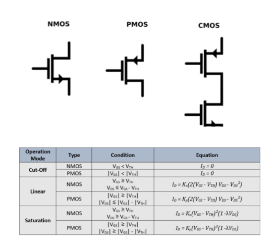
Integrated circuits (ICs) are composed of MOS transistors and are called MOS integrated circuits. ICs composed of NMOS transistors are specifically called NMOS integrated circuits; ICs composed of PMOS transistors are called PMOS integrated circuits. The circuit composed of NMOS and PMOS transistors is called a complementary MOS (CMOS) circuit.
In summary, an NMOS transistor is characterized by the use of n-type dopants in the gate region, leading to the creation of an inversion layer that enables or disables the flow of current between the source and drain terminals based on the applied gate voltage. This switching capability makes NMOS transistors essential components in digital circuits, serving roles such as amplification, logic operations, and memory storage in various electronic devices.
The symbol for an NMOS (n-channel metal-oxide-semiconductor) transistor is a standardized representation used in circuit diagrams to depict its essential terminals and characteristics.
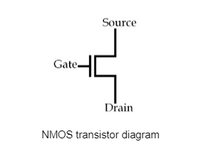
G: Gate
S: Source
D: Drain
The arrow pointing away from the source terminal indicates the direction of conventional current flow when the NMOS transistor is in the on-state (conducting). The arrow is consistent with the direction of electron flow, which is from the source to the drain.
In the realm of constructing waveforms for human-computer interaction, it becomes imperative to acknowledge the necessity for two distinct types of waveforms: 'high enable' and 'low enable.' As such, there exist two variations of NMOS switch circuits designed to cater to these specific waveform requirements. One configuration produces a 'low enable' waveform, wherein the signal is at a low level when the switch is pressed, while the other configuration generates a 'high enable' waveform, characterized by a high signal level when the switch is pressed.
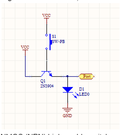
NMOS (NPN) high enable switch
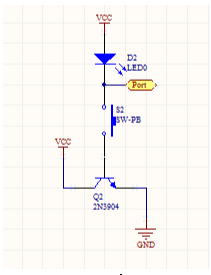
NMOS (NPN) low enable switch
The current flowing through an NMOS (n-channel metal-oxide-semiconductor) transistor can be described by the following basic equation, commonly known as the Saturation Region NMOS Current Equation:
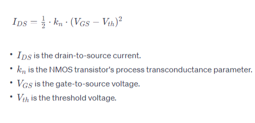
This equation applies specifically when the NMOS transistor is in the saturation region. In this region, the transistor is operating as a voltage-controlled current source. The threshold voltage represents the minimum gate-to-source voltage required to create a conductive channel between the source and drain terminals.
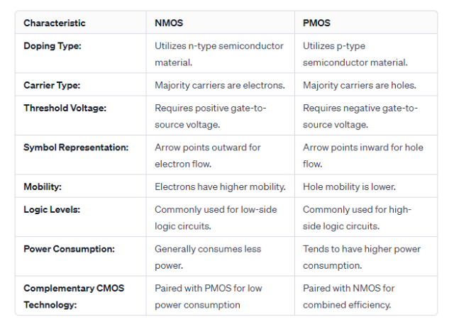
NMOS (n-channel metal-oxide-semiconductor) and PMOS (p-channel metal-oxide-semiconductor) transistors are two complementary types of MOSFETs (metal-oxide-semiconductor field-effect transistors) used in integrated circuit design. They have several key differences based on their construction, behavior, and electrical characteristics.
NMOS: Utilizes n-type (negatively doped) semiconductor material in the channel region beneath the gate.
PMOS: Utilizes p-type (positively doped) semiconductor material in the channel region beneath the gate.
NMOS: Majority carriers are electrons.
PMOS: Majority carriers are holes (positively charged carriers).
NMOS: Requires a positive gate-to-source voltage to create an inversion layer and allow electron flow. Threshold voltage is typically positive.
PMOS: Requires a negative gate-to-source voltage to create an inversion layer and allow hole flow. Threshold voltage is typically negative.
NMOS: The arrow in the symbol points outward from the source terminal, indicating the direction of electron flow.
PMOS: The arrow in the symbol points inward toward the source terminal, indicating the direction of hole flow.
NMOS: Electrons have higher mobility than holes in semiconductor materials, leading to generally faster electron-based devices.
PMOS: Hole mobility is lower than electron mobility, impacting the speed of PMOS devices compared to NMOS devices.
NMOS: Commonly used for the low side of logic circuits. Outputs high when the NMOS transistor is off (open circuit).
PMOS: Commonly used for the high side of logic circuits. Outputs high when the PMOS transistor is off.
NMOS: Generally consumes less power compared to PMOS due to the higher electron mobility and lower threshold voltage.
PMOS: Tends to have higher power consumption, especially in complementary CMOS designs.
NMOS: Paired with PMOS transistors in complementary CMOS (complementary metal-oxide-semiconductor) technology to achieve low power consumption and improved noise margins.
PMOS: Paired with NMOS transistors in complementary CMOS technology to benefit from the strengths of both types.
A depletion mode NMOS (n-channel metal-oxide-semiconductor) transistor is a type of MOSFET (metal-oxide-semiconductor field-effect transistor) that operates in a mode where the channel is naturally present and conductive in the absence of an applied gate voltage. Unlike enhancement mode NMOS transistors, which require a positive gate voltage to create an inversion layer and allow current flow, depletion mode NMOS transistors have a conductive channel by default.
An NMOS (n-channel metal-oxide-semiconductor) enhancement mode transistor is a type of MOSFET (metal-oxide-semiconductor field-effect transistor) that operates in a mode where an external voltage must be applied to the gate terminal to create an inversion layer and allow current flow between the source and drain terminals.
An NMOS pass transistor is a specific configuration of an n-channel metal-oxide-semiconductor (NMOS) transistor used to facilitate the passage of signals from one circuit node to another. In the context of digital circuits, a pass transistor can act as a switch that either allows or blocks the flow of a signal based on the state of its control terminal.
NMOS transistors play a pivotal role in electronic circuits, exhibiting distinctive functional characteristics that influence their behavior and performance. Understanding these properties is crucial for designing and optimizing circuitry in various applications.
An NMOS transistor demonstrates a closed circuit behavior when subjected to a non-zero voltage. In this state, the connection between the source and drain terminals acts akin to a conductive wire.
Conversely, when the transistor receives a voltage of approximately 0V, it transitions into an open circuit state. This interrupts the connection between the source and drain terminals, causing current to flow from the gate terminal to the drain.
The power supply experiences a current influx when the NMOS transistor is in the closed circuit state, and a non-zero voltage is applied. This current flows from the gate terminal to the power supply.
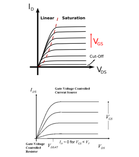
The current-voltage (I-V) properties of NMOS transistors are crucial for understanding their behavior. Two key voltages come into play: the voltage between the source and drain (VDS) and the voltage between the gate and source (VGS).
To analyze the I-V properties, a curve representing the relationship between the drain current (IDS) and VDS is obtained. This is achieved by grounding the terminals of the power supply, setting an initial VGS value, and incrementally stepping the VGS value from "0" to "VDD" to reach the highest DC voltage value.
At very low VGS values, IDS remains minimal, displaying a linear trend. As VGS increases, IDS undergoes enhancement, revealing intricate dependencies on both VGS and VDS.
The interplay between VGS and VDS significantly influences the performance of NMOS transistors. As VGS rises from low values, the drain current IDS experiences improvement, showcasing the transistor's ability to conduct more effectively.
The intricate relationship between VGS and VDS unfolds as the transistor progresses from the linear region to the saturation region. This transition is vital for optimizing the transistor's performance in different operational scenarios.
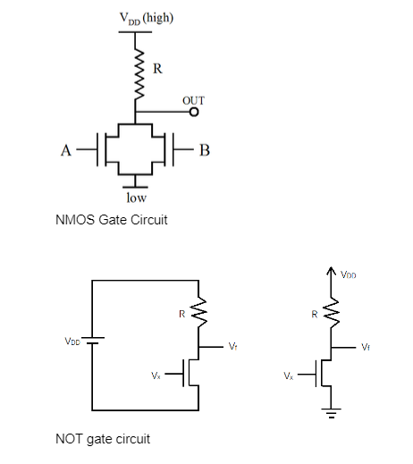
NMOS Gate Circuit
NOT gate circuit
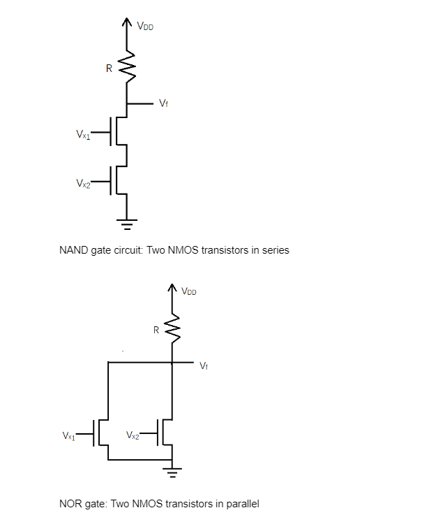
NAND gate circuit: Two NMOS transistors in series
NOR gate: Two NMOS transistors in parallel
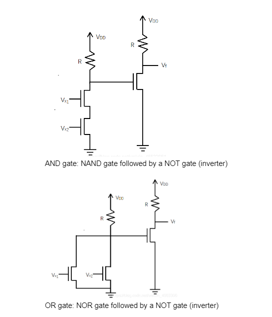
AND gate: NAND gate followed by a NOT gate (inverter)
OR gate: NOR gate followed by a NOT gate (inverter)
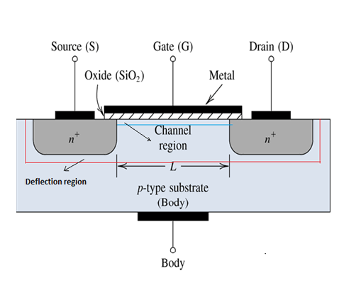
NMOS (n-channel metal-oxide-semiconductor) transistors function by manipulating the conductivity of a p-type semiconductor body through the creation of an inversion layer. The p-type material naturally lacks a conductive path between the source and drain terminals in its initial state. However, the transistor becomes conductive when a voltage is applied to the third terminal known as the gate.
Upon applying a voltage to the gate, an electric field is generated within the p-type material. This electric field attracts electrons towards the surface beneath the gate. As the gate voltage surpasses a specific threshold, it depletes the holes in the p-type material near the surface, leading to the creation of an excess of electrons and forming the inversion layer, also known as the n-channel.
The establishment of the n-channel provides a conductive path between the n-type source and drain terminals. Electrons can now flow from the source to the drain, allowing the transistor to conduct. The conductance of the transistor is directly controlled by the voltage applied to the gate. Higher gate voltages result in a wider and more conductive n-channel, enabling a greater flow of electrons.
Importantly, the transistor returns to its non-conductive state when the gate voltage falls below the threshold. This controlled behavior ensures that the transistor operates selectively, only conducting when a specific gate voltage is applied. In summary, the NMOS transistor's operation involves the intentional creation of an inversion layer in a p-type semiconductor, enabling precise control over its conductivity and functionality in electronic circuits.
The fabrication process of NMOS (n-channel metal-oxide-semiconductor) transistors involves several steps in the creation of the semiconductor device.
The process begins with the selection of a silicon wafer as the substrate. The silicon wafer is usually p-type, meaning it has an intrinsic positive charge.
The silicon wafer undergoes thorough cleaning to remove any contaminants and ensure a pristine surface for subsequent processing steps.
A thin layer of silicon dioxide (SiO2) is grown on the surface of the wafer through a process known as oxidation. This oxide layer acts as an insulator and is crucial for the formation of the transistor's gate dielectric.
A layer of photoresist is applied to the oxide layer, and a photomask is used to define the regions where the transistors' gates will be formed. The exposed areas are selectively etched to remove the oxide, leaving behind the patterned gate regions.
Dopants are introduced into the wafer to create the n-type regions for the source and drain terminals. This process is often achieved through ion implantation or diffusion. The patterned gate acts as a mask, defining the regions where the n-type dopants are introduced.
Insulating layers, such as silicon nitride (Si3N4) or additional layers of silicon dioxide, are deposited on the wafer to separate different layers and provide electrical isolation.
Openings, known as contacts, are created in the insulating layers above the source and drain regions. These openings allow for the formation of metal contacts that connect the transistor terminals to the external circuitry.
Metal layers, often aluminum or copper, are deposited and patterned to create metal interconnects that link various transistor terminals and form the conductive paths for electrical signals.
A passivation layer is applied to protect the transistor and metal layers from environmental factors, preventing contamination and ensuring long-term reliability.
The fabricated wafer undergoes extensive testing to verify the functionality of the NMOS transistors and ensure that they meet specified performance parameters.
The structure of an NMOS (n-channel metal-oxide-semiconductor) transistor is a fundamental element in semiconductor device design. It comprises various layers and regions that enable the transistor to control the flow of current between the source and drain terminals based on the voltage applied to the gate.
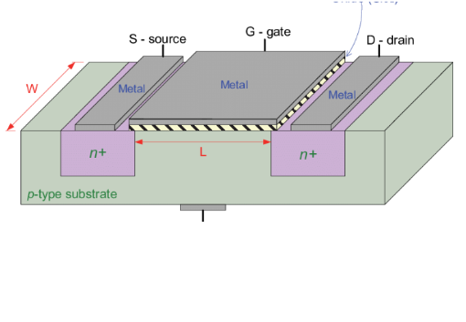
Substrate or Bulk
Oxide Layer (Gate Oxide)
Gate Terminal
Source and Drain Regions
Channel Region
Source and Drain Contacts
Interlayer Dielectrics
Metal Interconnects
The NMOS transistor structure is designed to control the flow of electrons from the source to the drain based on the voltage applied to the gate. By modulating the conductivity of the channel region beneath the gate, the transistor serves as a switch and amplifier in various electronic applications.