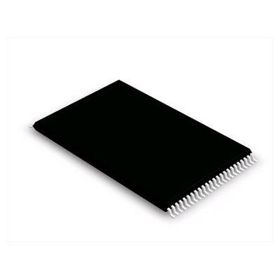
Buffer 2-CH Non-Inverting CMOS 6-Pin TSOP T/R


Les images sont fournies à titre indicatif.
Voir les spécifications du produit pour plus de détails sur le produit.
Buffer 2-CH Non-Inverting CMOS 6-Pin TSOP T/R
Les commandes de plus de 200 $ sont éligibles pour un cadeau de style chinois en édition limitée.
Les commandes de plus de 1 000 $ bénéficient d'une dispense des frais d'expédition de 30 $..
Les commandes supérieures à 5 000 $ bénéficient d'une exemption des frais d'expédition et de transaction..
Ces offres sont applicables aux nouveaux clients et aux clients existants et sont valables du 1er janvier 2024 au 31 décembre 2024..
NXP
74LVC2G34GV.125 datasheet
TSOP
Puces IC
 Lead free/RoHS Compliant
Soumettez votre demande de devis maintenant et nous espérons vous fournir un devis dans les délais mai 19, 2024. Passez votre commande maintenant et nous prévoyons de finaliser la transaction dans les mai 22, 2024. Ps : L’heure est conforme à GMT+8h00.


FEATURES
• Wide supply voltage range from 1.65 V to 5.5 V
• 5 V tolerant input/output for interfacing with 5 V logic
• High noise immunity
• Complies with JEDEC standard:
– JESD8-7 (1.65 V to 1.95 V)
– JESD8-5 (2.3 V to 2.7 V)
– JESD8B/JESD36 (2.7 V to 3.6 V).
• ESD protection:
– HBM EIA/JESD22-A114-B exceeds 2000 V
– MM EIA/JESD22-A115-A exceeds 200 V.
• ±24 mA output drive (VCC = 3.0 V)
• CMOS low power consumption
• Latch-up performance exceeds 250 mA
• Direct interface with TTL levels
• Multiple package options
• Specified from −40 °C to +85 °C and
−40 °C to +125 °C.
DESCRIPTION
The 74LVC2G34 is a high-performance, low-power,
low-voltage, Si-gate CMOS device and superior to most
advanced CMOS compatible TTL families.
Inputs can be driven from either 3.3 V or 5 V devices.
These feature allows the use of these devices as
translators in a mixed 3.3 V and 5 V environment.
This device is fully specified for partial power-down
applications using Ioff. The Ioff circuitry disables the output,
preventing the damaging backflow current through the
device when it is powered down.
The 74LVC2G34 provides two buffers.


Request a quote 74LVC2G34GV.125 at censtry.com. All items are new and original with 365 days warranty! The excellent quality
and guaranteed services of 74LVC2G34GV.125 in stock for sale, check stock quantity and pricing,
view product specifications, and order contact us:sales@censtry.com.
The price and lead time for 74LVC2G34GV.125 depending on the quantity required, please send your request to us,
our sales team will provide you price and delivery within 24 hours, we sincerely look forward to cooperating with you.
Deltron
2835 PCS
486-261612-68 .PDF
Deltron
6335 PCS
480-C070 .PDF
Deltron
3642 PCS
630-0700 .PDF
Deltron
6463 PCS
4DR3522 .PDF
2024-05-18
original IC, very good!
2024-05-18
Thanks exactly what I needed
2024-05-17
ok, parfait
2024-05-16
MUY BUENO , PROBADO . ATTE EL CHE FULL FUENTES LIMA PERU
2024-05-14
excellent product and quality of 1,000
2024-05-10
You will have a great order with Velocity.
2024-05-02
We never had any problem with Kamaka. Always smooth transactions in both direction
2024-04-16
We are pleased to cooperate with you .You are the good sale person of China !Wish our working together once more .
2024-03-15
Very professional, looking forward to doing much more business in the future.
2024-01-11
Very good customer Service,recommended !
Nous apprécions grandement vos commentaires. Veuillez partager votre avis le plus authentique.
*Veuillez vous connecter à votre compte avant de publier un commentaire